Guest |
Login
version 2.1.0
Manx – a catalogue of online computer manuals
Search
News
About
Help
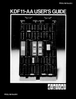
KDF11-AA User's Guide
Company:
Digital Equipment Corporation
Part:
EK-KDF11-UG-PR2
Date:
1979-03
Keywords:
M8186
Table of Contents
Chapter 1
Specifications
1.1
Introduction
1.2
Features
1.3
Specifications
1.4
Processor Hardware
1.4.1
General-Purpose Registers
1.4.2
Bus Cycles
1.4.3
Addressing Memory and Peripherals
1.4.4
Memory Management
1.4.5
Processor Status Word (PS)
1.4.5.1
Condition Codes (PS bits <3:0>)
1.4.5.2
Trace Bit (PS bit 4)
1.4.5.3
Priority Level (PS bits <7:5>)
1.4.5.4
Suspended Instruction (SI) (PS bit 8)
1.4.5.5
Previous Mode (PS bits <13:12>)
1.4.5.6
Current Mode (PS bits <15:14>)
1.5
Instruction Set
1.6
Floating Point Option
1.7
Memories and Peripherals
1.8
Related Documents
Chapter 2
Installation
2.1
Introduction
2.2
Jumper Configurations
2.2.1
Master Clock -- W1
2.2.2
Event Line -- W4
2.2.3
Power-Up Mode Selection -- W5 and W6
2.2.3.1
Power-Up Mode 0
2.2.3.2
Power-Up Mode 1
2.2.3.3
Power-Up Mode 2
2.2.3.4
Power-Up Mode 3
2.2.4
Halt/Trap Option -- W7
2.2.5
Starting Address 173000₈ -- W8
2.2.6
Selectable Starting Address -- W9 through W15
2.3
Module Contact Finger Identification
2.4
Backplane Pin Assignments and Their KDF11-AA Utilization
2.5
Hardware Options
2.5.1
Backplanes
2.5.1.1
H9270 Backplane
2.5.1.2
H9273-A Backplane
2.5.1.3
H9281 Backplane
2.5.1.4
DDV11-B Backplane
2.5.1.5
Device Priority Within Backplanes
2.5.2
Power Supplies
2.5.3
Enclosures
2.5.4
Memory Modules
2.5.5
Peripheral Options
2.6
System Differences
2.7
Module Installation Procedure
Chapter 3
Console ODT
3.1
Introduction
3.2
Terminal Interface
3.2.1
Receiver Control and Status Register (RCSR)
3.2.2
Receiver Buffer Register (RBUF)
3.2.3
Transmitter Control and Status Register (XCSR)
3.2.4
Transmitter Buffer Register (XBUF)
3.3
Console ODT Operation
3.3.1
Console ODT Entry Conditions
3.3.2
Console ODT Input Sequence
3.3.3
Console ODT Output Sequence
3.4
Console ODT Command Set
3.4.1
/ (ASCII 057) Slash
3.4.2
<CR> (ASCII 15) Carriage Return
3.4.3
<LF> (ASCII 12) Line Feed
3.4.4
$ (ASCII 044) or R (ASCII 122) Internal Register Designator
3.4.5
S (ASCII 123) Processor Status Word
3.4.6
G (ASCII 107) Go
3.4.7
P (ASCII 120) Proceed
3.4.8
Control-Shift-S (ASCII 23) Binary Dump
3.4.9
Reserved Commands
3.5
Address Specification
3.5.1
Processor I/O Addresses
3.5.2
Stack Pointer Selection
3.6
Entering of Octal Digits
3.7
ODT Timeout
3.8
Invalid Characters
Chapter 4
LSI-11 Bus
4.1
Introduction
4.2
Data Transfer Bus Cycles
4.2.1
Bus Cycle Protocol
4.2.1.1
Device Addressing
4.2.1.2
DATI
4.2.1.3
DATO(B)
4.2.1.4
DATIO(B)
4.2.2
Parity Protocol
4.3
Direct Memory Access
4.4
Interrupts
4.4.1
Device Priority
4.4.2
Interrupt Protocol
4.4.3
4-Level Interrupt Configurations
4.5
Control Functions
4.5.1
Memory Refresh
4.5.2
Halt
4.5.3
Initialization
4.5.4
Power Status
4.6
Bus Electrical Characteristics
4.6.1
Signal Level Specification
4.6.2
AC Load Definition
4.6.3
DC Load Definition
4.6.4
120 Ohm LSI-11 Bus
4.6.5
Bus Drivers
4.6.6
Bus Receivers
4.6.7
Bus Termination
4.6.8
Bus Interconnecting Wiring
4.6.8.1
Backplane Wiring
4.6.8.2
Intra-Backplane Bus Wiring
4.6.8.3
Power and Ground
4.6.8.4
Maintenance and Spare Pins
4.7
System Configurations
4.7.1
Rules for Configuring Single Backplane Systems
4.7.2
Rules for Configuring Multiple Backplane Systems
4.7.3
Power Supply Loading
Chapter 5
Processor Functional Description
5.1
Introduction
5.2
Data Chip
5.3
Control Chip
5.4
MMU Chip
5.5
Data-Address Lines (DAL)
5.6
Microinstruction Bus (MIB)
5.6.1
MIB15/Memory Management Enable (MME)
5.6.2
MIB14/Initialize (INIT F)
5.6.3
MIB13/Interrupt Acknowledge (IAK)
5.6.4
MIB12, 9, 8/Address-Input-Output (AIO) Codes
5.6.4.1
BUS CYC H
5.6.4.2
SYNC/DMA ENA H
5.6.5
MIB03/GPO 3
5.6.6
MIB02, 01, 00/GPO 2, 1, 0
5.7
BSYNC L Logic
5.8
Direct Memory Access (DMA)
5.8.1
DMA Logic
5.8.2
DMA Latency
5.9
Clock Generator Circuitry
5.9.1
Initialization
5.9.2
Wake-Up Circuit
5.9.3
Single-Step Circuit
5.10
Clock Generator Cycles
5.10.1
Normal Cycle
5.10.2
Clock Stutter Cycle
5.10.3
Clock Stop Cycle
5.10.4
Memory Management Cycle
5.10.5
Reset Cycle
Chapter 6
Addressing Modes
6.1
Introduction
6.2
Instruction Formats
6.3
Addressing Modes
6.3.1
Register Mode
6.3.2
Register Deferred Mode
6.3.3
Autoincrement Mode
6.3.4
Autoincrement Deferred Mode
6.3.5
Autodecrement Mode
6.3.6
Autodecrement Deferred Mode
6.3.7
Index Mode
6.3.8
Index Deferred Mode
6.3.9
Use of the PC as a General Register
6.3.9.1
PC Immediate Mode
6.3.9.2
PC Absolute Mode
6.3.9.3
PC Relative Mode
6.3.9.4
PC Relative Deferred Mode
6.3.10
Direct Addressing Modes Summary
6.3.11
Indirect Addressing Modes Summary
6.3.12
PC Register Addressing Modes Summary
6.3.13
Graphic Summary of Addressing Modes
Chapter 7
Instruction Set
7.1
Introduction
7.1.1
Single Operand Instructions
7.1.2
Double Operand Instructions
7.1.2.1
Double Operand Instruction Format
7.1.2.2
Byte Instructions
7.1.3
Program Control Instructions
7.1.3.1
Branch Instructions
7.1.3.2
Jump and Subroutine Instructions
7.1.3.3
Condition Code Instructions
7.1.3.4
Miscellaneous Instructions
7.1.4
Examples
7.1.4.1
Single Operand Instruction Example
7.1.4.2
Double Operand Instruction Example
7.1.4.3
Branch Instruction Example
7.2
Instruction Set
Chapter 8
Memory Management
8.1
Introduction
8.1.1
Programming
8.1.2
Basic Addressing
8.1.3
Active Page Registers
8.1.4
Capabilities Provided by Memory Management
8.2
Memory Relocation
8.2.1
Program Relocation
8.2.2
Memory Units
8.3
Protection
8.3.1
Inaccessible Memory
8.3.2
Read-Only Memory
8.3.3
Multiple Address Space
8.3.3.1
Mode Specification in Processor Status Word
8.3.3.2
Processor Status Word Protection
8.3.3.3
User Mode Restrictions
8.3.3.4
Interrupt and Trap Processing
8.4
Page Address Register (PAR)
8.5
Page Description Register (PDR)
8.5.1
Access Control Field (ACF)
8.5.2
Expansion Direction (ED)
8.5.3
Written Into (WI)
8.5.4
Page Length Field (PLF)
8.5.4.1
PLF For an Upward-Expandable Page
8.5.4.2
PLF For a Downward-Expandable Page
8.6
Virtual and Physical Addresses
8.6.1
Construction of a Physical Address
8.6.2
Determining the Program Physical Address
8.7
Status Registers
8.7.1
Status Register 0 (SR0)
8.7.1.1
Halt Nonresident
8.7.1.2
Halt Page Length
8.7.1.3
Halt Read Only
8.7.1.4
Mode of Operation
8.7.1.5
Page Number
8.7.1.6
Enable Relocation and Protection
8.7.2
Status Register 1 (SR1)
8.7.3
Status Register 2 (SR2)
8.7.4
Status Register 3 (SR3)
8.8
Memory Management Instructions
8.9
Programming Examples
Chapter 9
Floating Point
9.1
Introduction
9.2
Floating Point Data Formats
9.2.1
Nonvanishing Floating Point Numbers
9.2.2
Floating Point Zero
9.2.3
The Undefined Variable
9.2.4
Floating Point Data
9.3
Floating Point Status Register (FPS)
9.4
Floating Exception Code and Address Registers
9.5
Floating Point Processor Instruction Addressing
9.6
Accuracy
9.7
Floating Point Instructions
Chapter 10
Programming Techniques
10.1
Introduction
10.2
Position-Independent Code
10.2.1
Use of Addressing Modes in the Construction of Position-Independent Code
10.2.2
Position-Dependent/Position-Independent Comparative Example
10.3
Stacks
10.3.1
Pushing Onto a Stack
10.3.2
Popping From a Stack
10.3.3
Deleting Items From a Stack
10.3.4
Stack Uses
10.3.5
Stack Use Examples
10.3.6
Subroutine Linkage
10.3.6.1
Return from a Subroutine
10.3.6.2
Subroutine Advantages
10.3.7
Interrupts
10.3.7.1
Interrupt Service Routines
10.3.7.2
Nesting
10.3.8
Reentrancy
10.3.8.1
Reentrant Code
10.3.8.2
Writing Reentrant Code
10.3.9
Coroutines
10.3.9.1
Coroutine Calls
10.3.9.2
Coroutines Versus Subroutines
10.3.9.3
Using Coroutines
10.3.10
Recursion
10.3.11
Processor Traps
10.3.11.1
Trap Instructions
10.3.11.2
Use of Macro Calls
10.3.12
Conversion Routines
10.4
Programming the Processor Status Word
10.5
Programming Peripherals
10.6
PDP-11 Programming Examples
10.7
Looping Techniques
Appendix A
General Reference Information
Appendix B
Instruction Timing
Appendix C
KDF11/PDP-11 Program and Operation Difference
Appendix D
Integrated Circuits
Appendix E
Bootstrap Programs (Console Entry)
Appendix F
ODT Differences
Appendix G
KD11-F/KD11-HA/KDF11-AA Detailed Comparison
Appendix H
Parity on the LSI-11 Bus
Copies
Address:
http://bitsavers.org/pdf/dec/pdp11/1123/EK-KDF11-UG-PR2_Mar79.pdf
Site:
Al Kossow's Bitsavers
Format:
PDF
Size:
14798029 bytes (14.1 MiB)
MD5:
72c41fe50a74848fcb24d7067b3e39e2
Mirrors:
http://bitsavers.trailing-edge.com/pdf/dec/pdp11/1123/EK-KDF11-UG-PR2_Mar79.pdf
http://www.bighole.nl/pub/mirror/www.bitsavers.org/pdf/dec/pdp11/1123/EK-KDF11-UG-PR2_Mar79.pdf
http://www.mirrorservice.org/sites/www.bitsavers.org/pdf/dec/pdp11/1123/EK-KDF11-UG-PR2_Mar79.pdf
http://bitsavers.informatik.uni-stuttgart.de/pdf/dec/pdp11/1123/EK-KDF11-UG-PR2_Mar79.pdf
ftp://bitsavers.informatik.uni-stuttgart.de/pdf/dec/pdp11/1123/EK-KDF11-UG-PR2_Mar79.pdf
ftp://ftp.mirrorservice.org/sites/www.bitsavers.org/pdf/dec/pdp11/1123/EK-KDF11-UG-PR2_Mar79.pdf